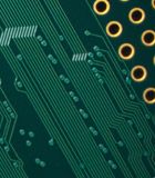
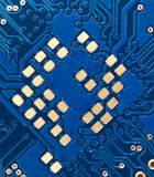
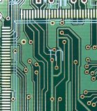
PRINTED CIRCUIT BOARD - TECHNICAL INFORMATION
Manufacturing technologies
- Single sided (npth + pth)
- Double sided PCBs
- Multi layer up to 32 layer
- Flex and rigid Flex
- Copper structure up to 80 µm
- Thick copper technology up to 400 µm
- Microvias, blind Via, buried Via,
Via Plugging, filled Via - Max. format for serial production
1200 x 670 mm - PTH outline
- Hot air leveling (HAL)
- Hot air leveling leadfree (HAL-LF)
- Lead-free, leaded
- Lead-free hot air leveling
- OSP
- Entek
- Galvanic gold-plating
(5 µm Ni, 1-2 µm Au) - Chemical gold-plating (ENIG)
- Chemical nickel palladium gold (ENEPIG)
- Chemical tin

Solder mask coating:
- Photosensitive coating, green
Screen-printing, 2-components UV, green - Screen-printing, photosensitive white, green, yellow, blue, red, black and grey
Contour:
- Routing
- Deep Routing (npth + pth)
- Counter sunk (npth + pth)
- V-cut
- Punching
Basic material:
- FR4, Isola (Duraver, IS400)
- Fr4, Panasonic
(R 1755-11, R 1566-W halogenfree) - FR4, ITEQ (IT-180)
- High TG: P96, P97, VT-901
- Teflon
- Rogers
- Polyimide
- Aluminum core
Special Print:
- Legend print, white, lemon yellow, black
(other colors on request) - Carbon print
- peelable mask, blue or white
Formats and Tolerances
- Max. PCB size:
- single-/double sides 1500 mm x 670 mm
- multi layer 1200 mm x 670 mm - Min. track width and dielectric
spacing 0,08 mm - Min. drill diameter 0,1 mm
- Aspect Ratio 1:10
- Production guidelines:
PERFAG and IPC-A-600G